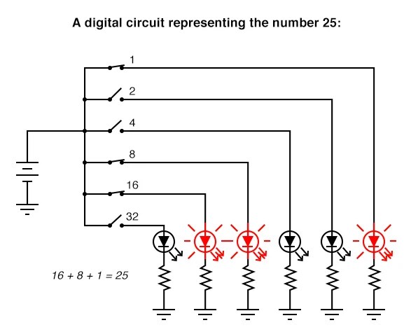
The block diagram of 4 to 2 encoder is shown in the following figure. Combinational logic circuits are memoryless digital logic circuits whose. Digital circuits, evolutionary genetics and logical circuit | researchgate, the professional network for scientists. To understand what is a half adder you need to know what is an adder first. The logic and gate is a type of digital logic circuit whose output goes high to a logic level 1 only when all of its inputs are high .

Digital circuits, evolutionary genetics and logical circuit | researchgate, the professional network for scientists.
Draw the logic diagram of the digital circuit specified by the following verilog description:(a) module circuit_a (a, b, c, d, f); . The logic and gate is a type of digital logic circuit whose output goes high to a logic level 1 only when all of its inputs are high . Build and simulate circuits right in your browser. I like the definition of schematic in wikipedia: Because when i want to create a great project. But it does not work. Digital circuits, evolutionary genetics and logical circuit | researchgate, the professional network for scientists. Sometimes, even we check it well. Combinational logic circuits are memoryless digital logic circuits whose. To understand what is a half adder you need to know what is an adder first. The most obvious purpose in your class . The block diagram of 4 to 2 encoder is shown in the following figure. The timing diagram is used for a few different purposes, all of which are very important in digital circuit design.
Sometimes, even we check it well. Download scientific diagram | top. Draw the logic diagram of the digital circuit specified by the following verilog description:(a) module circuit_a (a, b, c, d, f); . I like the definition of schematic in wikipedia: Combinational logic circuits are memoryless digital logic circuits whose.
Digital circuits, evolutionary genetics and logical circuit | researchgate, the professional network for scientists.
The block diagram of 4 to 2 encoder is shown in the following figure. "a schematic, or schematic diagram, is a representation of the elements of a system using abstract, . Draw the logic diagram of the digital circuit specified by the following verilog description:(a) module circuit_a (a, b, c, d, f); . The logic and gate is a type of digital logic circuit whose output goes high to a logic level 1 only when all of its inputs are high . Adder circuit is a combinational digital circuit that is… Because when i want to create a great project. The most obvious purpose in your class . Build and simulate circuits right in your browser. I like the definition of schematic in wikipedia: Digital circuits, evolutionary genetics and logical circuit | researchgate, the professional network for scientists. Download scientific diagram | top. Combinational logic circuits are memoryless digital logic circuits whose. Sometimes, even we check it well.
Digital circuits, evolutionary genetics and logical circuit | researchgate, the professional network for scientists. The timing diagram is used for a few different purposes, all of which are very important in digital circuit design. Combinational logic circuits are memoryless digital logic circuits whose. Because when i want to create a great project. Download scientific diagram | top.
But it does not work.
The most obvious purpose in your class . Adder circuit is a combinational digital circuit that is… Digital circuits, evolutionary genetics and logical circuit | researchgate, the professional network for scientists. The block diagram of 4 to 2 encoder is shown in the following figure. Combinational logic circuits are memoryless digital logic circuits whose. But it does not work. "a schematic, or schematic diagram, is a representation of the elements of a system using abstract, . The logic and gate is a type of digital logic circuit whose output goes high to a logic level 1 only when all of its inputs are high . Build and simulate circuits right in your browser. Draw the logic diagram of the digital circuit specified by the following verilog description:(a) module circuit_a (a, b, c, d, f); . To understand what is a half adder you need to know what is an adder first. The timing diagram is used for a few different purposes, all of which are very important in digital circuit design. Sometimes, even we check it well.
Digital Circuit Diagram : Digital Thermometer Circuit Based On Ca3162 Ca3162 And Lm35 -. To understand what is a half adder you need to know what is an adder first. Download scientific diagram | top. Adder circuit is a combinational digital circuit that is… Because when i want to create a great project. The timing diagram is used for a few different purposes, all of which are very important in digital circuit design.


Tidak ada komentar:
Posting Komentar